
Can FEL Disrupt ASML's EUV Monopoly? The Future of Light Sources in a 3D Era
As the semiconductor industry transitions into GAA transistors, backside power delivery, and 3D packaging, the role of the light source is quietly shifting.

ASML's dominance in EUV through Cymer's LPP (Laser Produced Plasma) source has fueled 2D scaling through 7nm, 5nm, and into 3nm. But with lithography patterns becoming more critical rather than more frequent, and 3D integration displacing planar scaling, can an alternative like the Free Electron Laser (FEL) find its moment?

Why Higher EUV Power Matters
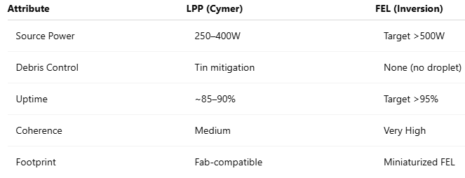
EUV throughput is directly tied to source power. Today’s LPP systems operate around 250–350W, enabling 140–160 wafers per hour. Scaling this to >500W could push throughput beyond 220 wafers/hour, significantly reducing cost per layer. More power also supports High-NA EUV systems (~0.55 NA), which suffer from photon losses due to increased optical complexity.
ASML’s EUV Roadmap: Stable But Constrained
ASML continues to extend its roadmap with:
NXE:3800E (0.33 NA, ~400W) for 2nm
EXE:5000/5200 (0.55 NA, 500–600W target) for 1.4nm and beyond
But all rely on the same core: Cymer's CO2 LPP source, which has issues with tin debris, mirror degradation, and uptime (~85–90%).
Enter FEL: Clean, Coherent, and Powerful
Free Electron Lasers (FEL) generate EUV by accelerating electrons through undulators, producing ultra-coherent, tunable light. FELs eliminate debris, extend mirror life, and offer potential for >500W of scalable power. Companies like Inversion Semiconductor are miniaturizing FELs to fit fab environments and decouple EUV from ASML’s closed ecosystem.
Why ASML Hasn’t Adopted FEL (Yet)
Despite its advantages, FEL adoption by ASML faces hurdles:
Size and integration complexity
Lack of proven fab-grade uptime
Disruption to ASML’s Cymer-aligned hardware/software stack
High R&D and qualification cost
Still, if FELs hit 500W+ with 95% uptime and fab-friendly size by 2027–28, ASML could be forced to consider them—either via partnership or acquisition.
Cost Targets for FEL to Compete
To realistically replace LPP, FEL needs to:
Reduce capex per unit to <$35M (vs. $40–50M for LPP)
Cut operating cost by >50% (no tin, longer optics life)
Bring EUV cost per wafer layer below $80 (currently $100–120 with LPP)
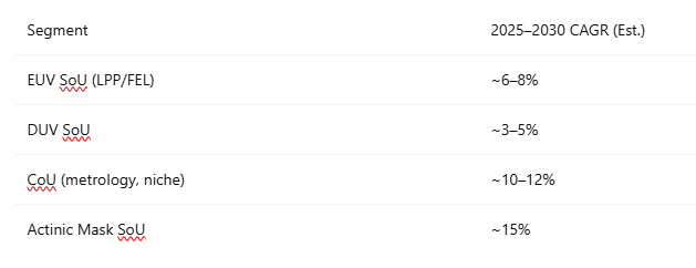
How the SoU Market Will Evolve in a 3D Era
As transistor scaling plateaus, SoU demand will shift:
Fewer 2D layers → fewer total litho steps per transistor
But increased complexity per layer (e.g., GAA fins, BSPD vias)
Growth in 3D packaging, actinic inspection, and backside layers
Final Thoughts
FEL-based EUV sources won’t replace LPP overnight—but they offer a compelling long-term path. In a world where 3D and hybr
id integration take center stage, light sources must evolve from brute force power to precision, coherence, and uptime. If Inversion or a peer succeeds in delivering a compact, fab-ready FEL with stable 500W+ output, the EUV landscape—and ASML’s monopoly—could shift dramatically.
Subscribe for more insights into lithography, packaging, and the future of semiconductor infrastructure.